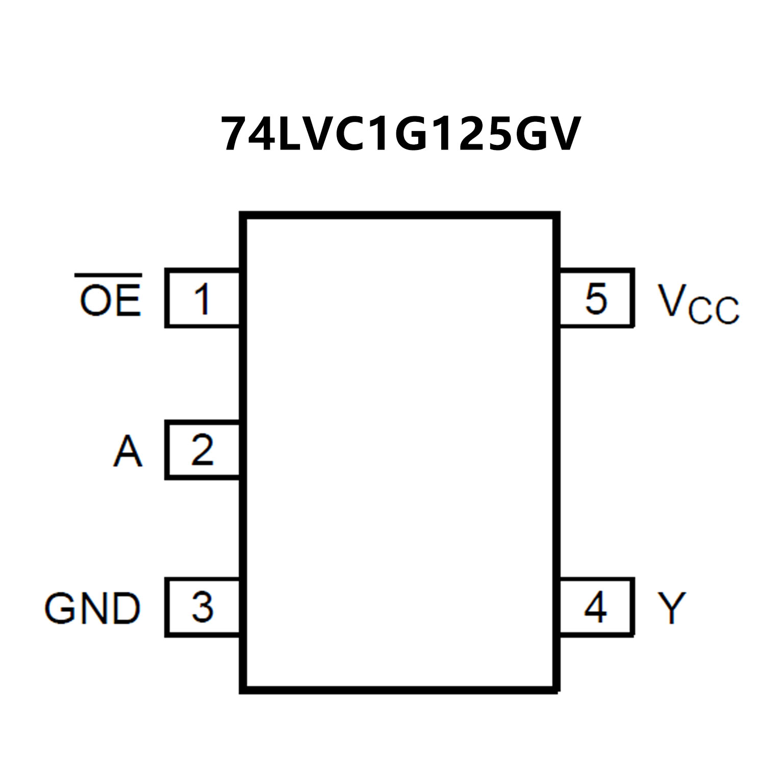


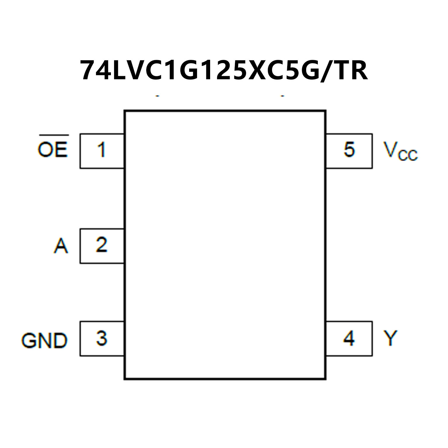
 74LVC1G125.pdf
? Wide Supply Voltage Range: 1.65V to 5.5V
? High Noise Immunity
? ±24mA Output Drive at VCC = 3.0V
? CMOS Low Power Consumption
? Inputs Accept Voltages Up to 5V
? Direct Interface with TTL Levels
? -40℃ to +125℃ Operating Temperature Range
? Available in a Green SC70-5 Package
? Wide supply voltage range from 1.65 V to 5.5 V
? Overvoltage tolerant inputs to 5.5 V
? High noise immunity ? CMOS low power consumption
? IOFF circuitry provides partial Power-down mode operation
? ±24 mA output drive (VCC = 3.0 V)
? Latch-up performance exceeds 250 mA
? Direct interface with TTL levels
? Complies with JEDEC standards:
JESD8-7 (1.65 V to 1.95 V)
JESD8-5 (2.3 V to 2.7 V)
JESD8C (2.7 V to 3.6 V)
JESD36 (4.5 V to 5.5 V)
? ESD protection:
HBM JESD22-A114F exceeds 2000 V
MM JESD22-A115-A exceeds 200 V
? Multiple package options
? Specified from -40 °C to +85 °C and -40 °C to +125 °C