


 SGM48524A.pdf
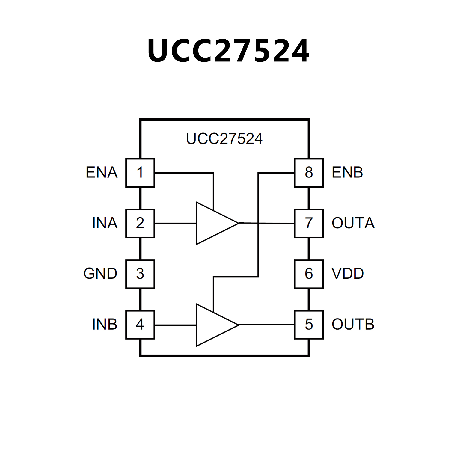
? Two Independent Gate Drive Channels
? 4.5V to 18V Single Supply Range (VDD)
? 5A Peak Source/Sink Pulse Current Drive
? Independent Enable Pin for Each Channel
? TTL and CMOS Compatible Logic Threshold
? Logic Levels Independent of Supply Voltage
? Hysteretic Input Logic for High Noise Immunity
? Outputs are Logic Low when Inputs are Floating
? Negative Voltage Handling Capability:
-8V DC at Inputs
-2V, 200ns Pulse for Outputs (OUTx)
? Glitch-Free Operation at Power-Up and Power-
? Down: Outputs Pulled Low during Supply UVLO
? Fast Propagation Delays: 18ns (TYP)
? Fast Rise Time: 8ns (TYP)
? Fast Fall Time: 8ns (TYP)
? Delay Matching between Two Channels: 1ns (TYP)
? Channels can be Paralleled for Higher Drive Current
-40℃ to +140℃ Operating Temperature Range
? Packaging:
SGM48523/4A/5 Available in Green SOIC-8,
MSOP-8 (Exposed Pad) and TDFN-3×3-8L Packages
SGM48526 Available in a Green TDFN-3×3-8L Package
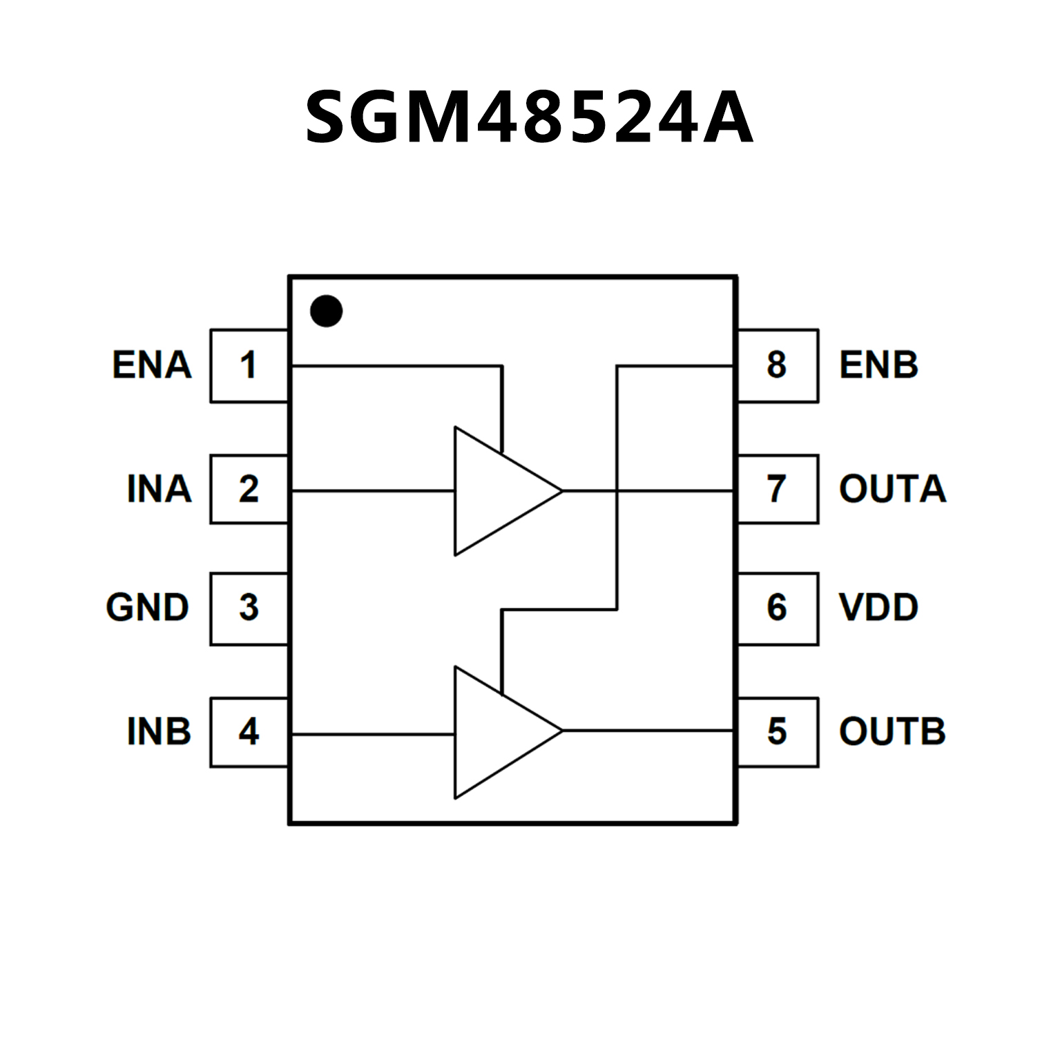
? 工业标准引脚分配
? 两个独立的栅极驱动通道
? 5A峰值驱动源电流和灌电流
? 针对每个输出的独立使能功能
? 与电源电压无关的TTL和CMOS兼容逻辑阀值针对高抗扰度的滯后逻辑阀值
? 输入和使能引脚电压电平不受VDD引脚偏置电源电压限制
? 4.5V至18V单电源范围
? 在VDD欠压闭锁(UVLO)期间,输出保持低电平,(以确保加电和断电时的无毛刺脉冲运行)
? 快速传播延迟( 典型值13ns)
? 快速上升和下降时间( 典型值7ns和6ns)
? 两通道间典型值为1ns的延迟匹配时间
? 针对更高的驱动电流,两个输出可以并联
? 当输入悬空时输出保持在低电平
? 环氧树脂双列直插式(PDIP)-8,小外形尺寸集成电路(SOIC)-8,表面贴装小外形尺寸(MSOP)-8封装 PowerPADTM和3mm x 3mm超薄型小外形尺寸(WSON)-8封装选项
? -40°C 至+140°C的运行温度范围